

Adam Awale, On-device research, AGI Inc., PhD candidate, MPS Lab, Arizona State University (advisor: Prof. Aviral Shrivastava)
Processing-Near-Memory is a technology in which compute units sit physically next to the memory cells. The result is higher effective bandwidth: instead of shipping data across the chip to a distant processor, those units operate on it where it already sits, so the same power budget buys more computation. For edge devices balancing latency, area, and battery, that tradeoff is critical.
The industry has moved fast in the last year:
This is the trajectory that edge compute is on.
A terminology note. "In-memory" means compute before the sense amplifier, inside the DRAM. "Near-memory" means compute after the sense amplifier. People use the terms interchangeably and shouldn't: only the in-vs-near distinction actually matters, because it changes the technology stack underneath. The "processing" vs "compute" prefix is purely cosmetic.
PNM is the industry's most promising answer to the data movement challenge.
At AGI, Inc. data movement is also the problem we solve every day. The agents we ship act across any app, on phones, cars, and wearables; what limits the model on those devices is memory, bandwidth, and power, not the compute. How well an agent runs comes down to how efficient the dataflows are.
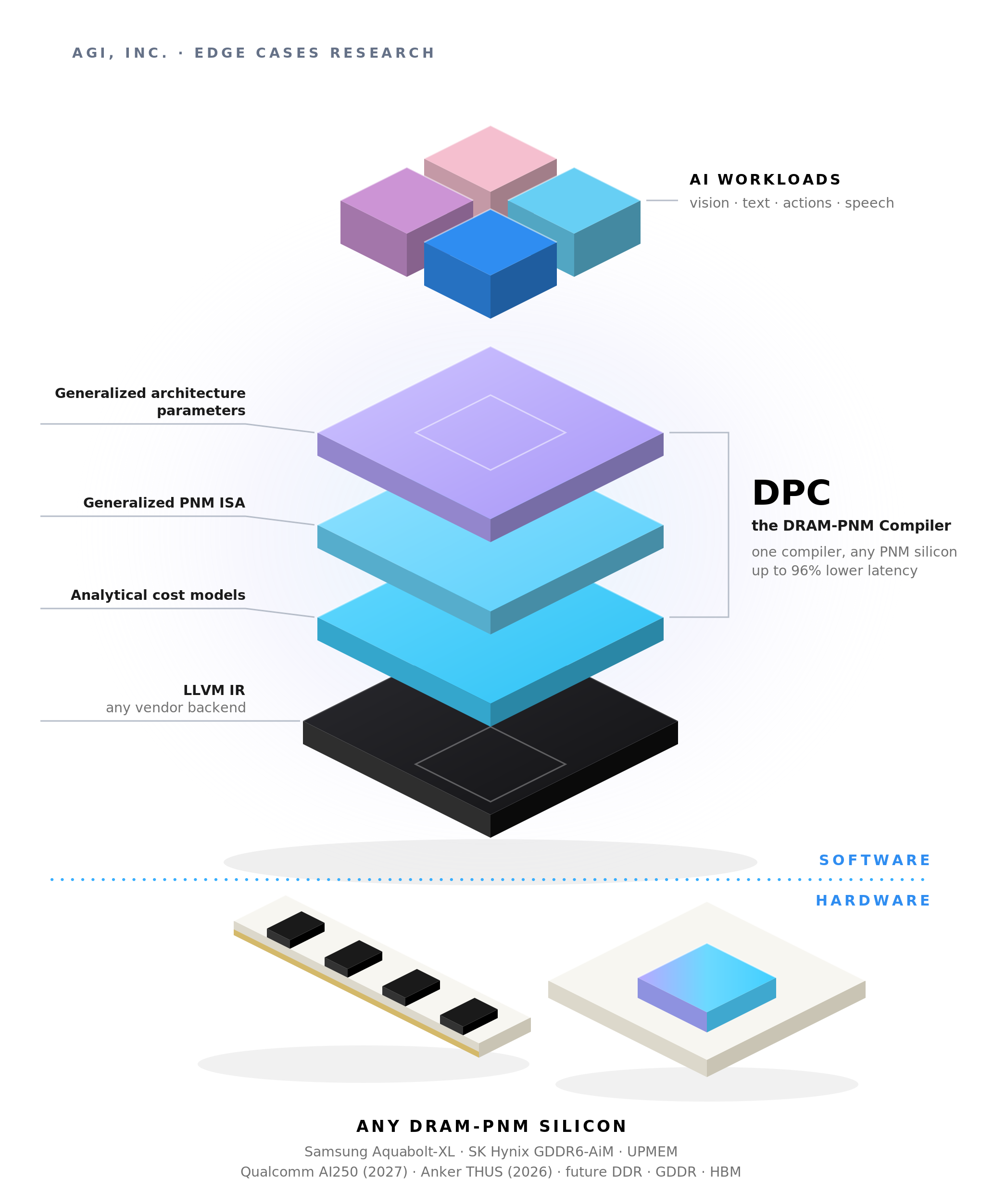
Adam Awale on our on-device research team spent his PhD solving this problem, with Prof. Aviral Shrivastava at MPS Lab at Arizona State. The result is DPC, a compilation framework that gets optimal performance out of any DRAM-PNM architecture, where every previous attempt was tied to one chip or one workload.
At AGI we build upon this same cost-model-driven approach to map our models onto the silicon we already ship on: optimize the workload first, fit it to each device's memory via cost models, tune for the specific hardware last - which allows us to deliver the fastest inference on edge hardware that transfers from chip to chip.
That's our answer to one of the hardest scaling problems in on-device AI, because every device maker runs different silicon: supporting a new device becomes a mapping problem, not a rebuild. It's how we get the most out of the hardware that exists now, and why the same stack will be ready on day one when PNM chips ship in volume.
There are two reasons:
DRAM standards are over twenty years old, and adding compute without breaking memory-controller compatibility has historically been hard. Transistor scaling has finally made it tractable, which is why prototype silicon is appearing now.
As we mentioned above, the second reason is the compiler. Most production frameworks today (LLVM, MLIR, NVCC, MLX) were built for CPUs, GPUs, and NPUs, and PNM is a fundamentally different architecture. The scheduling and mapping heuristics that work there don't transfer, and until that gets rethought, PNM hardware doesn't reach consumers.
Existing PNM work falls into three buckets, none of which solve the general problem:
DPC (the DRAM-PNM Compiler) addresses the aforementioned issues.
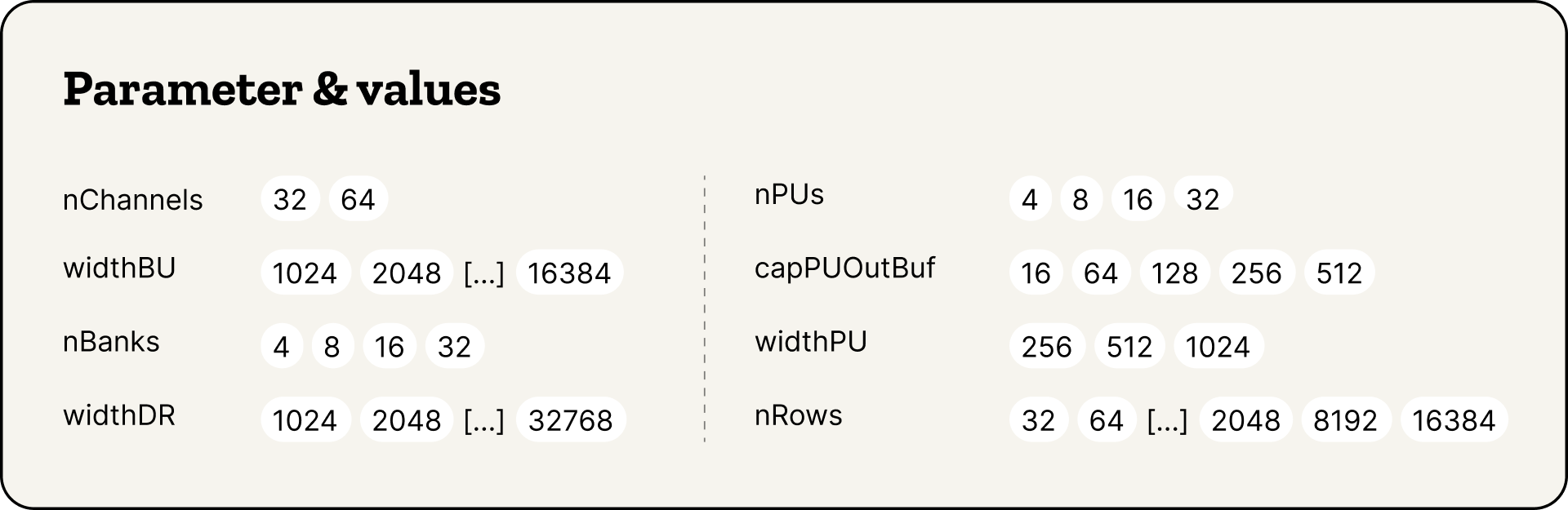
Developed by Adam Awale and Prof. Aviral Shrivastava in the MPS Lab at Arizona State University, DPC treats mapping as a global optimization problem rather than a hand-tuning exercise. For a given target, it constructs a pruned design space defined by the architecture's parameters, its PNM ISA, and the affine workload, then iteratively searches that space, scoring each candidate point with analytical cost models, to find the set of optimizations that sits at the global cost minimum outlined in figure 2.
Three pieces:
Workload scope: Affine programs (loops of the form AX + B). That covers matrix multiplication, matrix-vector multiplication, and element-wise operations, which is most of what a transformer or CNN does at inference.
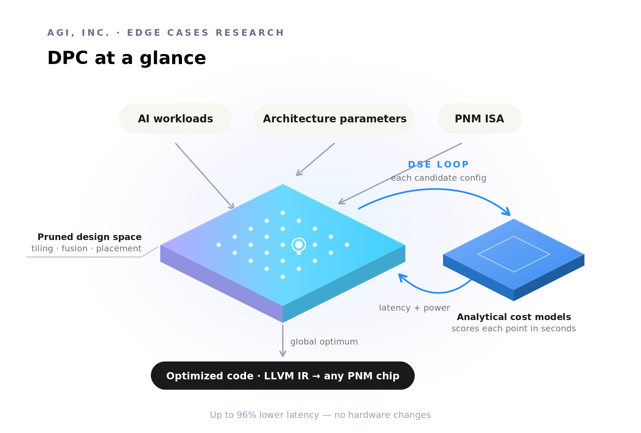
DPC was benchmarked against the hand-tuned compilers shipped with Samsung Aquabolt-XL (PIMSimulator) and SK Hynix AiM (aim_simulator), using both vendors' cycle-accurate simulators.
Workloads: DORN, GPT2, LSTM, RNN, StarGAN, ResNet, ViT.
Before reporting performance numbers, DPC's analytical cost model was validated against both vendors' cycle-accurate simulators on GEMV across multiple dimensions. All deltas were zero, constant, or negligible at scale. That's the bar for using an analytical model to drive design-space exploration.
Head-to-head on native architectures. DPC beats both native compilers on the hardware they were designed for. Samsung Aquabolt-XL: average 67.42% latency improvement, max 96.42% (ResNet). SK Hynix AiM: average 18.9% improvement, max 87.82% (ResNet). The SK Hynix gap is smaller because their architecture uses a cheap SRAM buffer for the operations where DPC's optimizations apply, so there's less cost for the compiler to shave off.

DPC architecture sweep
On DDR architectures: average latency reduction 36.54%, max 95.3%.
On HBM architectures: average latency 80.76%, up to 89.74%. The same compiler holds across the design space, not just at one operating point.
.png)
.png)
On DDR architectures: average power improvement 4.03% (same BU-cost reason as above).
On HBM architectures: average 84.36%.
.png)
No hardware changes. Every number above is from compilation alone: memory placement, instruction selection, design-space search. The silicon stays identical.
The paper is currently under peer review. Code release will follow acceptance. The open-source simulators DPC builds on are publicly available: Samsung's PIMSimulator and SK Hynix's AiM Simulator.
The next milestone for DPC is LLVM lowering for the first commercial PNM silicon that ships. The ISA is designed to lower into LLVM IR for any backend, so when real PNM hardware reaches developers, the compilation path will be ready.
Beyond DPC, the broader question is whether the industry catches up on the compiler side fast enough to match the silicon. PNM chips arrive in 2027 whether their toolchains are ready or not. The interesting work over the next 18 months is everything in the gap between announcement and a developer actually getting useful throughput out of one.
Today's consensus in on-device AI: quantize aggressively, throw the model onto the NPU, hope it runs fast. On high-end devices with generous power budgets, fine. On the edge, it falls apart. Heterogeneous compilation, putting the right computation on the right unit, with memory placement that doesn't waste cycles moving data, is what actually gets the latency down at low power. Quantization is a band-aid on top of an unsolved problem.
Look at the history. Vector instructions started as specialized accelerator hardware. So did VLIW. Both are standard in every CPU and GPU now. Compute-near-memory is at the same point in that arc today: vendor-specific, hard to program, niche.
Same pattern. Within five years, every edge device will ship with some form of compute-near-memory. The vendors will keep changing the name. The architecture is settled. The compilers are not.
The next five years of edge compute will be defined by hardware-software co-design at the memory layer, not another round of quantization tricks. PNM is the first concrete instance of that shift. The compiler is what's gating it.
Our research series on on-device AI, compilers, and edge inference.
We're hiring on-device research talent. If the problems in this post are the problems you work on, check out our open roles.
Open-source simulators
Prior compilation work
Industry announcements
PNM startup ecosystem
Academic
The DPC paper is currently under peer review. Code release will follow acceptance.